Making a boost converter
Background
As described in the previous post in 2022, I made a simple buck converter controlled by a Raspberry Pi. After some drama happened with its SD card, I migrated the entire circuit to my brand new RPi Pico with some slight modifications. To make the circuit run on pure 5V, I added a cheap boost board before my circuit to generate 20V.
For those around me, these things all happened during and after the Great Power Outage of 2022, in which I had to run everything on a 6V lead-acid battery. Therefore, this buck-boost-buck topology had been bugging me from day one: it is terrible in terms of efficiency and EM interference. I had always wanted to make my own boost converter instead. However, it scares me that “theoretically” this circuit will be capable of generating an infinite voltage. Do I need to add closed-loop feedback for it? What if I miscalculated and it fries my Pico?
This week I finally ran some SPICE models and decided to get my hands dirty.
Design
I am not actually designing the topology from scratch. I took the one on Wikipedia and simply chose the components based on my needs.
The first problem was that I could not get anything higher than 7V with the RJK1536DPN I took off. I felt like there could be two possible reasons: either the on-resistance was too high, or the gate voltage was too low. I tried both, and it turned out that the gate voltage was the problem. Fortunately, I still had five IRL520N MOSFETs with a gate threshold voltage of 2V. It worked like a charm and gave me 9.2V without tuning anything else.

I also included a voltage divider on the output to measure the voltage with the Pico’s ADC in this diagram. I have not physically implemented it yet though.
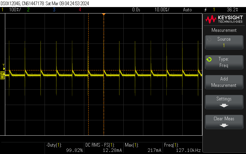
The rest was pretty much just controlling the PWM signal. By trial and error on the breadboard, I found that a frequency of around 125kHz generated the highest voltage. I also swapped the inductor to one I took from another dead switch-mode power supply.
The next thing that worried me was that this circuit cannot be turned off: even when the PWM duty cycle is 0, the load will still see 5V. However, my measurements showed that the light bulb only drew some microamps at this state, so I decided to leave it as it was.
Finally, I cannot leave the MOSFET on constantly: at this state, we are essentially shorting the 5V supply at steady state. For now, this is done on the software side. Maybe I should add something else to the circuit to prevent this from happening.
Results
I did these measurements on my Mac’s USB port, which definitely did not try to provide a constant voltage.
When switching at 60kHz, 58% duty cycle, I got 60mA@14.2V with an input of 0.415A@4.8V. That is a terrible efficiency of 43%. At 125kHz, 58% duty cycle, I got 72mA@13.12V with an input of just 0.227A@4.9V. Now the efficiency is a whopping 85%.
Again I studied the relationship between the output voltage and the duty cycle on the completed circuit. This one was able to reach a higher voltage of 40V, probably because the finished circuit has much lower resistance than my rusty breadboard plus jumper wires setup.
However, the data was still weird, probably because the input voltage was not constant. I will try to do this again with a more stable power supply.
 Note:
This time, the duty cycle is out of 1000.
The light turns on at around 21.
Note:
This time, the duty cycle is out of 1000.
The light turns on at around 21.
Reflection
I was surprised by how high the efficiency was, even just on the breadboard. I used to be surprised at the efficiencies shown in those SMPS IC datasheets, but now I feel like maybe it is just a matter of choosing the right components. Also, I am using a discrete MOSFET instead of one crammed in a tiny package, so the loss and heat dissipation are much better. In fact, the MOSFET was barely warm after running for a while (except for the time I accidentally left the gate high).
A boost converter definitely comes with more responsibilities than a buck converter. In fact, the last two data points on the graph were already outside of the light bulb’s rating, voltage-wise. Maybe I should add a feedback loop. Since the circuit is always working with the same load, I am simply limiting the duty cycle to 530 out of 1000. It works for now.
Update (2024-03-08)
Today, I did a more “proper” test with a regulated supply. The input voltage had a range of 5.22V to 5.28V.
Two interesting results that happened in both tests:
- This circuit has some kind of a hysteresis behaviour around 42% duty cycle:
- If I start low from an output of below 9.1V (duty cycle below 37%) and step up the duty cycle across 42%, the voltage jumps from 9V to 12V.
- If it enters this 37% to 42% region when the duty cycle is already above 37%, the output voltage curve is smooth.
- There is an output dip at around 58% duty cycle.
I suspect that both of these are because of the interaction with the (very nonlinear) load.
I do not plan to test again with a constant load though… I just want to make an ASIC (haha).

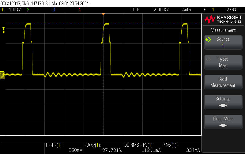
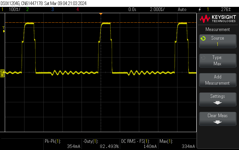
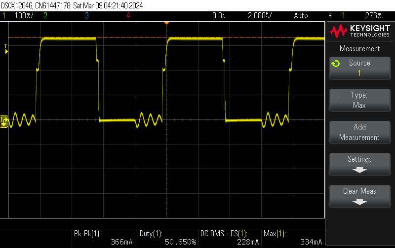
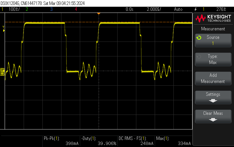
I also used our lab’s nice oscilloscope to measure the gate signal and the output. I forgot to set the mode, so although it shows a vertical division of 100mA, it actually means 1V.
What I cannot explain is the gate ringing. It is probably not the result of resonance on the gate, because the ringing does not immediately begin after an edge: it actually always terminates at the rising edge. Its initial amplitude also increases with the duty cycle, instead of being constant like the rising or falling time. This probably means it is related to the MOSFET and the load. The ringing can bring the gate voltage to below -0.5V after the duty cycle exceeds 50%, which exceeds the absolute maximum rating of the Pico’s GPIO pin. I need to try to fix this when I have time.
The output ripple at 53% duty cycle was around 0.36V. The spikes of around 3.3V are a bigger worry.
Gate signal at 10% duty cycle
Gate signal at 15% duty cycle
Gate signal at 47% duty cycle
Gate signal at 58% duty cycle
Output at 53% duty cycle (AC coupling)